Implementing a MMC/SD/SDIO stack using CAM framework(Part 2)
Hi, In the next part lets look at other files which makes up the SDIO stack within mmccam framework. Please have a look at previous part for more info: http://81.4.107.225/wordpress/index.php/2018/03/19/implementing-a-mmc-sd-sdio-stack-using-cam-framework/
mmc_sdio.c
sdio_fill_mmcio_rw_direct is basically a wrapper for CMD_52 that's needed to read/write directly into mmc register R5. Remember that register R5 in mmc, is used for RCA(Relative card address) management. It's right time now to talk about different command types of SD/MMC/SDIO:
CMD_53 is of ac type. where address of 8bit opcode is provided by adr,
Note:- For those who don't understand open drain mode,
Output pins can be configured in 3 ways,
[caption id="" align="alignright" width="272"]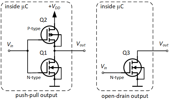 Source: https://os.mbed.com/media/uploads/tbjazic/05outputs.png[/caption]
Open drain is power efficient and Push pull mode is very fast!! so, SD card initialization id done in open drain mode and then push-pull mode takes over during cmd/data transfer.
Input Pins can be connected in 4 ways:
Now, to understand the above function, one should know about all the macros. Below, is the file to refer to in that case:
Now, look at SD_IO_RW_DIRECT its a class 9 command type for directly read and write in SDIO card case. Then, there is SD_IO_RW_FUNC ( #define SD_IO_RW_FUNC(x) (((x) & 0x7) << 28) ) it takes a uint8 type value extracts it's 7th bit and shift that bit to 28 position. then, SD_IO_RW_ADR ( #define SD_IO_RW_ADR(x) (((x) & 0x1FFFF) << 9) ) takes a 32 bit address takes it's first 16 its shift it by 9 bit i.e [25:9] and sends it to SD card to take set these 16 bits as it's RCA. SD_IO_RW_WR sets 1 at 31 position which indicates write operation. SD_IO_RW_RAW sets 1 at 27 position indicating raw data to be exchanged. SD_IO_RW_DAT takes 8 bit of data and put it in beginning of the packet . #define MMC_RSP_R5 (MMC_RSP_PRESENT | MMC_RSP_CRC | MMC_RSP_OPCODE) MMC_RSP_R5 sets the CRC and opcode of the command. MMC_CMD_AC shows that it's an address only command no data will be transferred.
sdio_parse_mmcio_rw_direct function is pretty straight forward, it's used to parse the response header indicating any CRC error or any other error reported by mmc card.
mmc_xpt.c
First two structure and character array are just a list of different functions that can be performed on mmc and SDIO card as of now.
Then we have mmc_dev_async function which as explained in previous post, is used to handle any asynchronous interrupt from CAM bus, in case of hot plug/hot unplug. It detects the device, and registers it accordingly on CAM bus.
Notice, here the keyword 'LUN' it refers to Logical Unit Number a storage device has. So, CAM_TARGET_WILDCARD and CAM_LUN_WILDCARD makes sure that device is a valid storage/IO device.
mmc_scan_lun basically check the Logical Unit Numbers of the device. CAM_LUN_WILDCARD only checks whether LUN == 0 or not. Each device has LUN = 0 even if it has multiple logical units , it's a bit confusing, but it looks like device registers other LUNs only after one of it's LUN gets attached. Source: here
mmc_action() is pretty straightforward. It calls xpt_action() after handling several standard cases. It also calls mmc_scan_lun if needed.
mmc_announce_periph is called upon confirmation of connection to any new device. notice that it creates a CCB and then initializes it with xpt_action.
Then, mmcprobe_register registers a new device on the CAM bus. only after registration, it can be associated with a CCB.
Next, important function is mmcprobe_start
Notice the switch case statement here, which converts a I/O command to it's SCSI equivalent. That is with just the name of the command it associates all the register value corresponding to it.
Few other supporting files are left. I'll update this post with there details as well
References:
mmc_sdio.c
+void sdio_fill_mmcio_rw_direct(union ccb *ccb, uint8_t f, uint8_t wr, uint32_t adr, uint8_t *data) {
+        struct ccb_mmcio *mmcio;
+
+	CAM_DEBUG(ccb->ccb_h.path, CAM_DEBUG_TRACE,
+		  ("sdio_fill_mmcio(f=%d, wr=%d, adr=%02x, data=%02x)\n", f, wr, adr, (data == NULL ? 0 : *data)));
+	mmcio = &ccb->mmcio;
+
+        mmcio->cmd.opcode = SD_IO_RW_DIRECT;
+        mmcio->cmd.arg = SD_IO_RW_FUNC(f) | SD_IO_RW_ADR(adr);
+        if (wr)
+                mmcio->cmd.arg |= SD_IO_RW_WR | SD_IO_RW_RAW | SD_IO_RW_DAT(*data);
+        mmcio->cmd.flags = MMC_RSP_R5 | MMC_CMD_AC;
+        mmcio->cmd.data->len = 0;
+}
sdio_fill_mmcio_rw_direct is basically a wrapper for CMD_52 that's needed to read/write directly into mmc register R5. Remember that register R5 in mmc, is used for RCA(Relative card address) management. It's right time now to talk about different command types of SD/MMC/SDIO:
- broadcast commands (bc), no response
- broadcast commands with response (bcr) (Note: No open drain on SD card)
- addressed (point-to-point) commands (ac), no data transfer on DAT lines
- addressed (point-to-point) data transfer commands (adtc), data transfer on DAT lines
CMD_53 is of ac type. where address of 8bit opcode is provided by adr,
Note:- For those who don't understand open drain mode,
Output pins can be configured in 3 ways,
[caption id="" align="alignright" width="272"]
Source: https://os.mbed.com/media/uploads/tbjazic/05outputs.png[/caption]- open drain - a transistor connects to low and nothing else
- open drain, with pull-up - a transistor connects to low, and a resistor connects to high
- push-pull - a transistor connects to high, and a transistor connects to low (only one is operated at a time)
Open drain is power efficient and Push pull mode is very fast!! so, SD card initialization id done in open drain mode and then push-pull mode takes over during cmd/data transfer.
Input Pins can be connected in 4 ways:
- pull-up - a resistor connected to high
- pull-down - a resistor connected to low
- pull-up and pull-down - both a resistor connected to high and a resistor connected to low (only useful in rare cases).
- Schmitt triggered input mode
Now, to understand the above function, one should know about all the macros. Below, is the file to refer to in that case:
/*
 * This file contains the register definitions for the mmc and sd buses.
 * They are taken from publicly available sources.
 */

struct mmc_data;
struct mmc_request;

struct mmc_command {
	uint32_t	opcode;
	uint32_t	arg;
	uint32_t	resp[4];
	uint32_t	flags;		/* Expected responses */
#define	MMC_RSP_PRESENT	(1ul << 0)	/* Response */
#define	MMC_RSP_136	(1ul << 1)	/* 136 bit response */
#define	MMC_RSP_CRC	(1ul << 2)	/* Expect valid crc */
#define	MMC_RSP_BUSY	(1ul << 3)	/* Card may send busy */
#define	MMC_RSP_OPCODE	(1ul << 4)	/* Response include opcode */
#define	MMC_RSP_MASK	0x1ful
#define	MMC_CMD_AC	(0ul << 5)	/* Addressed Command, no data */
#define	MMC_CMD_ADTC	(1ul << 5)	/* Addressed Data transfer cmd */
#define	MMC_CMD_BC	(2ul << 5)	/* Broadcast command, no response */
#define	MMC_CMD_BCR	(3ul << 5)	/* Broadcast command with response */
#define	MMC_CMD_MASK	(3ul << 5)

/* Possible response types defined in the standard: */
#define	MMC_RSP_NONE	(0)
#define	MMC_RSP_R1	(MMC_RSP_PRESENT | MMC_RSP_CRC | MMC_RSP_OPCODE)
#define	MMC_RSP_R1B	(MMC_RSP_PRESENT | MMC_RSP_CRC | MMC_RSP_OPCODE | MMC_RSP_BUSY)
#define	MMC_RSP_R2	(MMC_RSP_PRESENT | MMC_RSP_136 | MMC_RSP_CRC)
#define	MMC_RSP_R3	(MMC_RSP_PRESENT)
#define	MMC_RSP_R4	(MMC_RSP_PRESENT)
#define	MMC_RSP_R5	(MMC_RSP_PRESENT | MMC_RSP_CRC | MMC_RSP_OPCODE)
#define	MMC_RSP_R5B	(MMC_RSP_PRESENT | MMC_RSP_CRC | MMC_RSP_OPCODE | MMC_RSP_BUSY)
#define	MMC_RSP_R6	(MMC_RSP_PRESENT | MMC_RSP_CRC | MMC_RSP_OPCODE)
#define	MMC_RSP_R7	(MMC_RSP_PRESENT | MMC_RSP_CRC | MMC_RSP_OPCODE)
#define	MMC_RSP(x)	((x) & MMC_RSP_MASK)
	uint32_t	retries;
	uint32_t	error;
#define	MMC_ERR_NONE	0
#define	MMC_ERR_TIMEOUT	1
#define	MMC_ERR_BADCRC	2
#define	MMC_ERR_FIFO	3
#define	MMC_ERR_FAILED	4
#define	MMC_ERR_INVALID	5
#define	MMC_ERR_NO_MEMORY 6
#define	MMC_ERR_MAX	6
	struct mmc_data	*data;		/* Data segment with cmd */
	struct mmc_request *mrq;	/* backpointer to request */
};

/*
 * R1 responses
 *
 * Types (per SD 2.0 standard)
 *	e : error bit
 *	s : status bit
 *	r : detected and set for the actual command response
 *	x : Detected and set during command execution.  The host can get
 *	    the status by issuing a command with R1 response.
 *
 * Clear Condition (per SD 2.0 standard)
 *	a : according to the card current state.
 *	b : always related to the previous command.  reception of a valid
 *	    command will clear it (with a delay of one command).
 *	c : clear by read
 */
#define	R1_OUT_OF_RANGE (1u << 31)		/* erx, c */
#define	R1_ADDRESS_ERROR (1u << 30)		/* erx, c */
#define	R1_BLOCK_LEN_ERROR (1u << 29)		/* erx, c */
#define	R1_ERASE_SEQ_ERROR (1u << 28)		/* er, c */
#define	R1_ERASE_PARAM (1u << 27)		/* erx, c */
#define	R1_WP_VIOLATION (1u << 26)		/* erx, c */
#define	R1_CARD_IS_LOCKED (1u << 25)		/* sx, a */
#define	R1_LOCK_UNLOCK_FAILED (1u << 24)	/* erx, c */
#define	R1_COM_CRC_ERROR (1u << 23)		/* er, b */
#define	R1_ILLEGAL_COMMAND (1u << 22)		/* er, b */
#define	R1_CARD_ECC_FAILED (1u << 21)		/* erx, c */
#define	R1_CC_ERROR (1u << 20)			/* erx, c */
#define	R1_ERROR (1u << 19)			/* erx, c */
#define	R1_CSD_OVERWRITE (1u << 16)		/* erx, c */
#define	R1_WP_ERASE_SKIP (1u << 15)		/* erx, c */
#define	R1_CARD_ECC_DISABLED (1u << 14)		/* sx, a */
#define	R1_ERASE_RESET (1u << 13)		/* sr, c */
#define	R1_CURRENT_STATE_MASK (0xfu << 9)	/* sx, b */
#define	R1_READY_FOR_DATA (1u << 8)		/* sx, a */
#define	R1_SWITCH_ERROR (1u << 7)		/* sx, c */
#define	R1_APP_CMD (1u << 5)			/* sr, c */
#define	R1_AKE_SEQ_ERROR (1u << 3)		/* er, c */
#define	R1_STATUS(x)		((x) & 0xFFFFE000)
#define	R1_CURRENT_STATE(x)	(((x) & R1_CURRENT_STATE_MASK) >> 9)
#define	R1_STATE_IDLE	0
#define	R1_STATE_READY	1
#define	R1_STATE_IDENT	2
#define	R1_STATE_STBY	3
#define	R1_STATE_TRAN	4
#define	R1_STATE_DATA	5
#define	R1_STATE_RCV	6
#define	R1_STATE_PRG	7
#define	R1_STATE_DIS	8

/* R4 response (SDIO) */
#define R4_IO_NUM_FUNCTIONS(ocr)	(((ocr) >> 28) & 0x3)
#define R4_IO_MEM_PRESENT		(0x1<<27)
#define R4_IO_OCR_MASK			0x00fffff0

/*
 * R5 responses
 *
 * Types (per SD 2.0 standard)
 *e : error bit
 *s : status bit
 *r : detected and set for the actual command response
 *x : Detected and set during command execution.  The host can get
 *    the status by issuing a command with R1 response.
 *
 * Clear Condition (per SD 2.0 standard)
 *a : according to the card current state.
 *b : always related to the previous command.  reception of a valid
 *    command will clear it (with a delay of one command).
 *c : clear by read
 */
#define R5_COM_CRC_ERROR		(1u << 15)/* er, b */
#define R5_ILLEGAL_COMMAND		(1u << 14)/* er, b */
#define R5_IO_CURRENT_STATE_MASK	(3u << 12)/* s, b */
#define R5_IO_CURRENT_STATE(x) 		(((x) & R5_IO_CURRENT_STATE_MASK) >> 12)
#define R5_ERROR			(1u << 11)/* erx, c */
#define R5_FUNCTION_NUMBER		(1u << 9)/* er, c */
#define R5_OUT_OF_RANGE			(1u << 8)/* er, c */
struct mmc_data {
	size_t len;		/* size of the data */
	size_t xfer_len;
	void *data;		/* data buffer */
	uint32_t	flags;
#define	MMC_DATA_WRITE	(1UL << 0)
#define	MMC_DATA_READ	(1UL << 1)
#define	MMC_DATA_STREAM	(1UL << 2)
#define	MMC_DATA_MULTI	(1UL << 3)
	struct mmc_request *mrq;
};

struct mmc_request {
	struct mmc_command *cmd;
	struct mmc_command *stop;
	void (*done)(struct mmc_request *); /* Completion function */
	void *done_data;		/* requestor set data */
	uint32_t flags;
#define	MMC_REQ_DONE	1
#define	MMC_TUNE_DONE	2
};

/* Command definitions */

/* Class 0 and 1: Basic commands & read stream commands */
#define	MMC_GO_IDLE_STATE	0
#define	MMC_SEND_OP_COND	1
#define	MMC_ALL_SEND_CID	2
#define	MMC_SET_RELATIVE_ADDR	3
#define	SD_SEND_RELATIVE_ADDR	3
#define	MMC_SET_DSR		4
#define	MMC_SLEEP_AWAKE		5
#define IO_SEND_OP_COND		5
#define	MMC_SWITCH_FUNC		6
#define	 MMC_SWITCH_FUNC_CMDS	 0
#define	 MMC_SWITCH_FUNC_SET	 1
#define	 MMC_SWITCH_FUNC_CLR	 2
#define	 MMC_SWITCH_FUNC_WR	 3
#define	MMC_SELECT_CARD		7
#define	MMC_DESELECT_CARD	7
#define	MMC_SEND_EXT_CSD	8
#define	SD_SEND_IF_COND		8
#define	MMC_SEND_CSD		9
#define	MMC_SEND_CID		10
#define	MMC_READ_DAT_UNTIL_STOP	11
#define	MMC_STOP_TRANSMISSION	12
#define	MMC_SEND_STATUS		13
#define	MMC_BUSTEST_R		14
#define	MMC_GO_INACTIVE_STATE	15
#define	MMC_BUSTEST_W		19

/* Class 2: Block oriented read commands */
#define	MMC_SET_BLOCKLEN	16
#define	MMC_READ_SINGLE_BLOCK	17
#define	MMC_READ_MULTIPLE_BLOCK	18
#define	MMC_SEND_TUNING_BLOCK	19
#define	MMC_SEND_TUNING_BLOCK_HS200 21

/* Class 3: Stream write commands */
#define	MMC_WRITE_DAT_UNTIL_STOP 20
			/* reserved: 22 */

/* Class 4: Block oriented write commands */
#define	MMC_SET_BLOCK_COUNT	23
#define	MMC_WRITE_BLOCK		24
#define	MMC_WRITE_MULTIPLE_BLOCK 25
#define	MMC_PROGARM_CID		26
#define	MMC_PROGRAM_CSD		27

/* Class 6: Block oriented write protection commands */
#define	MMC_SET_WRITE_PROT	28
#define	MMC_CLR_WRITE_PROT	29
#define	MMC_SEND_WRITE_PROT	30
			/* reserved: 31 */

/* Class 5: Erase commands */
#define	SD_ERASE_WR_BLK_START	32
#define	SD_ERASE_WR_BLK_END	33
			/* 34 -- reserved old command */
#define	MMC_ERASE_GROUP_START	35
#define	MMC_ERASE_GROUP_END	36
			/* 37 -- reserved old command */
#define	MMC_ERASE		38
#define	 MMC_ERASE_ERASE	0x00000000
#define	 MMC_ERASE_TRIM		0x00000001
#define	 MMC_ERASE_FULE		0x00000002
#define	 MMC_ERASE_DISCARD	0x00000003
#define	 MMC_ERASE_SECURE_ERASE	0x80000000
#define	 MMC_ERASE_SECURE_TRIM1	0x80000001
#define	 MMC_ERASE_SECURE_TRIM2	0x80008000

/* Class 9: I/O mode commands */
#define	MMC_FAST_IO		39
#define	MMC_GO_IRQ_STATE	40
			/* reserved: 41 */

/* Class 7: Lock card */
#define	MMC_LOCK_UNLOCK		42
			/* reserved: 43 */
			/* reserved: 44 */
			/* reserved: 45 */
			/* reserved: 46 */
			/* reserved: 47 */
			/* reserved: 48 */
			/* reserved: 49 */
			/* reserved: 50 */
			/* reserved: 51 */
			/* reserved: 54 */

/* Class 8: Application specific commands */
#define	MMC_APP_CMD		55
#define	MMC_GEN_CMD		56
			/* reserved: 57 */
			/* reserved: 58 */
			/* reserved: 59 */
			/* reserved for mfg: 60 */
			/* reserved for mfg: 61 */
			/* reserved for mfg: 62 */
			/* reserved for mfg: 63 */

/* Class 9: I/O cards (sd) */
#define	SD_IO_RW_DIRECT		52
/* CMD52 arguments */
#define  SD_ARG_CMD52_READ		(0<<31)
#define  SD_ARG_CMD52_WRITE		(1<<31)
#define  SD_ARG_CMD52_FUNC_SHIFT		28
#define  SD_ARG_CMD52_FUNC_MASK		0x7
#define  SD_ARG_CMD52_EXCHANGE		(1<<27)
#define  SD_ARG_CMD52_REG_SHIFT		9
#define  SD_ARG_CMD52_REG_MASK		0x1ffff
#define  SD_ARG_CMD52_DATA_SHIFT		0
#define  SD_ARG_CMD52_DATA_MASK		0xff
#define  SD_R5_DATA(resp)		((resp)[0] & 0xff)

#define	SD_IO_RW_EXTENDED	53
/* CMD53 arguments */
#define  SD_ARG_CMD53_READ		(0<<31)
#define  SD_ARG_CMD53_WRITE		(1<<31)
#define  SD_ARG_CMD53_FUNC_SHIFT		28
#define  SD_ARG_CMD53_FUNC_MASK		0x7
#define  SD_ARG_CMD53_BLOCK_MODE		(1<<27)
#define  SD_ARG_CMD53_INCREMENT		(1<<26)
#define  SD_ARG_CMD53_REG_SHIFT		9
#define  SD_ARG_CMD53_REG_MASK		0x1ffff
#define  SD_ARG_CMD53_LENGTH_SHIFT	0
#define  SD_ARG_CMD53_LENGTH_MASK	0x1ff
#define  SD_ARG_CMD53_LENGTH_MAX		64 /* XXX should be 511? */

/* Class 10: Switch function commands */
#define	SD_SWITCH_FUNC		6
			/* reserved: 34 */
			/* reserved: 35 */
			/* reserved: 36 */
			/* reserved: 37 */
			/* reserved: 50 */
			/* reserved: 57 */

/* Application specific commands for SD */
#define	ACMD_SET_BUS_WIDTH	6
#define	ACMD_SD_STATUS		13
#define	ACMD_SEND_NUM_WR_BLOCKS	22
#define	ACMD_SET_WR_BLK_ERASE_COUNT 23
#define	ACMD_SD_SEND_OP_COND	41
#define	ACMD_SET_CLR_CARD_DETECT 42
#define	ACMD_SEND_SCR		51

/*
 * EXT_CSD fields
 */
#define	EXT_CSD_EXT_PART_ATTR	52	/* R/W, 2 bytes */
#define	EXT_CSD_ENH_START_ADDR	136	/* R/W, 4 bytes */
#define	EXT_CSD_ENH_SIZE_MULT	140	/* R/W, 3 bytes */
#define	EXT_CSD_GP_SIZE_MULT	143	/* R/W, 12 bytes */
#define	EXT_CSD_PART_SET	155	/* R/W */
#define	EXT_CSD_PART_ATTR	156	/* R/W */
#define	EXT_CSD_PART_SUPPORT	160	/* RO */
#define	EXT_CSD_RPMB_MULT	168	/* RO */
#define	EXT_CSD_BOOT_WP_STATUS	174	/* RO */
#define	EXT_CSD_ERASE_GRP_DEF	175	/* R/W */
#define	EXT_CSD_PART_CONFIG	179	/* R/W */
#define	EXT_CSD_BUS_WIDTH	183	/* R/W */
#define	EXT_CSD_STROBE_SUPPORT	184	/* RO */
#define	EXT_CSD_HS_TIMING	185	/* R/W */
#define	EXT_CSD_POWER_CLASS	187	/* R/W */
#define	EXT_CSD_CARD_TYPE	196	/* RO */
#define	EXT_CSD_DRIVER_STRENGTH	197	/* RO */
#define	EXT_CSD_REV		192	/* RO */
#define	EXT_CSD_PART_SWITCH_TO	199	/* RO */
#define	EXT_CSD_PWR_CL_52_195	200	/* RO */
#define	EXT_CSD_PWR_CL_26_195	201	/* RO */
#define	EXT_CSD_PWR_CL_52_360	202	/* RO */
#define	EXT_CSD_PWR_CL_26_360	203	/* RO */
#define	EXT_CSD_SEC_CNT		212	/* RO, 4 bytes */
#define	EXT_CSD_HC_WP_GRP_SIZE	221	/* RO */
#define	EXT_CSD_ERASE_TO_MULT	223	/* RO */
#define	EXT_CSD_ERASE_GRP_SIZE	224	/* RO */
#define	EXT_CSD_BOOT_SIZE_MULT	226	/* RO */
#define	EXT_CSD_SEC_FEATURE_SUPPORT 231	/* RO */
#define	EXT_CSD_PWR_CL_200_195	236	/* RO */
#define	EXT_CSD_PWR_CL_200_360	237	/* RO */
#define	EXT_CSD_PWR_CL_52_195_DDR 238	/* RO */
#define	EXT_CSD_PWR_CL_52_360_DDR 239	/* RO */
#define	EXT_CSD_GEN_CMD6_TIME	248	/* RO */
#define	EXT_CSD_PWR_CL_200_360_DDR 253	/* RO */

/*
 * EXT_CSD field definitions
 */
#define	EXT_CSD_EXT_PART_ATTR_DEFAULT		0x0
#define	EXT_CSD_EXT_PART_ATTR_SYSTEMCODE	0x1
#define	EXT_CSD_EXT_PART_ATTR_NPERSISTENT	0x2

#define	EXT_CSD_PART_SET_COMPLETED		0x01

#define	EXT_CSD_PART_ATTR_ENH_USR		0x01
#define	EXT_CSD_PART_ATTR_ENH_GP0		0x02
#define	EXT_CSD_PART_ATTR_ENH_GP1		0x04
#define	EXT_CSD_PART_ATTR_ENH_GP2		0x08
#define	EXT_CSD_PART_ATTR_ENH_GP3		0x10
#define	EXT_CSD_PART_ATTR_ENH_MASK		0x1f

#define	EXT_CSD_PART_SUPPORT_EN			0x01
#define	EXT_CSD_PART_SUPPORT_ENH_ATTR_EN	0x02
#define	EXT_CSD_PART_SUPPORT_EXT_ATTR_EN	0x04

#define	EXT_CSD_BOOT_WP_STATUS_BOOT0_PWR	0x01
#define	EXT_CSD_BOOT_WP_STATUS_BOOT0_PERM	0x02
#define	EXT_CSD_BOOT_WP_STATUS_BOOT0_MASK	0x03
#define	EXT_CSD_BOOT_WP_STATUS_BOOT1_PWR	0x04
#define	EXT_CSD_BOOT_WP_STATUS_BOOT1_PERM	0x08
#define	EXT_CSD_BOOT_WP_STATUS_BOOT1_MASK	0x0c

#define	EXT_CSD_ERASE_GRP_DEF_EN	0x01

#define	EXT_CSD_PART_CONFIG_ACC_DEFAULT	0x00
#define	EXT_CSD_PART_CONFIG_ACC_BOOT0	0x01
#define	EXT_CSD_PART_CONFIG_ACC_BOOT1	0x02
#define	EXT_CSD_PART_CONFIG_ACC_RPMB	0x03
#define	EXT_CSD_PART_CONFIG_ACC_GP0	0x04
#define	EXT_CSD_PART_CONFIG_ACC_GP1	0x05
#define	EXT_CSD_PART_CONFIG_ACC_GP2	0x06
#define	EXT_CSD_PART_CONFIG_ACC_GP3	0x07
#define	EXT_CSD_PART_CONFIG_ACC_MASK	0x07
#define	EXT_CSD_PART_CONFIG_BOOT0	0x08
#define	EXT_CSD_PART_CONFIG_BOOT1	0x10
#define	EXT_CSD_PART_CONFIG_BOOT_USR	0x38
#define	EXT_CSD_PART_CONFIG_BOOT_MASK	0x38
#define	EXT_CSD_PART_CONFIG_BOOT_ACK	0x40

#define	EXT_CSD_CMD_SET_NORMAL		1
#define	EXT_CSD_CMD_SET_SECURE		2
#define	EXT_CSD_CMD_SET_CPSECURE	4

#define	EXT_CSD_HS_TIMING_BC		0
#define	EXT_CSD_HS_TIMING_HS		1
#define	EXT_CSD_HS_TIMING_HS200		2
#define	EXT_CSD_HS_TIMING_HS400		3
#define	EXT_CSD_HS_TIMING_DRV_STR_SHIFT	4

#define	EXT_CSD_POWER_CLASS_8BIT_MASK	0xf0
#define	EXT_CSD_POWER_CLASS_8BIT_SHIFT	4
#define	EXT_CSD_POWER_CLASS_4BIT_MASK	0x0f
#define	EXT_CSD_POWER_CLASS_4BIT_SHIFT	0

#define	EXT_CSD_CARD_TYPE_HS_26		0x0001
#define	EXT_CSD_CARD_TYPE_HS_52		0x0002
#define	EXT_CSD_CARD_TYPE_DDR_52_1_8V	0x0004
#define	EXT_CSD_CARD_TYPE_DDR_52_1_2V	0x0008
#define	EXT_CSD_CARD_TYPE_HS200_1_8V	0x0010
#define	EXT_CSD_CARD_TYPE_HS200_1_2V	0x0020
#define	EXT_CSD_CARD_TYPE_HS400_1_8V	0x0040
#define	EXT_CSD_CARD_TYPE_HS400_1_2V	0x0080

#define	EXT_CSD_BUS_WIDTH_1	0
#define	EXT_CSD_BUS_WIDTH_4	1
#define	EXT_CSD_BUS_WIDTH_8	2
#define	EXT_CSD_BUS_WIDTH_4_DDR	5
#define	EXT_CSD_BUS_WIDTH_8_DDR	6
#define	EXT_CSD_BUS_WIDTH_ES	0x80

#define	EXT_CSD_STROBE_SUPPORT_EN	0x01

#define	EXT_CSD_SEC_FEATURE_SUPPORT_ER_EN	0x01
#define	EXT_CSD_SEC_FEATURE_SUPPORT_BD_BLK_EN	0x04
#define	EXT_CSD_SEC_FEATURE_SUPPORT_GB_CL_EN	0x10
#define	EXT_CSD_SEC_FEATURE_SUPPORT_SANITIZE	0x40

/*
 * Vendor specific EXT_CSD fields
 */
/* SanDisk iNAND */
#define	EXT_CSD_INAND_CMD38			113
#define	 EXT_CSD_INAND_CMD38_ERASE		0x00
#define	 EXT_CSD_INAND_CMD38_TRIM		0x01
#define	 EXT_CSD_INAND_CMD38_SECURE_ERASE	0x80
#define	 EXT_CSD_INAND_CMD38_SECURE_TRIM1	0x81
#define	 EXT_CSD_INAND_CMD38_SECURE_TRIM2	0x82

#define	MMC_TYPE_HS_26_MAX		26000000
#define	MMC_TYPE_HS_52_MAX		52000000
#define	MMC_TYPE_DDR52_MAX		52000000
#define	MMC_TYPE_HS200_HS400ES_MAX	200000000

/*
 * SD bus widths
 */
#define	SD_BUS_WIDTH_1		0
#define	SD_BUS_WIDTH_4		2

/*
 * SD Switch
 */
#define	SD_SWITCH_MODE_CHECK	0
#define	SD_SWITCH_MODE_SET	1
#define	SD_SWITCH_GROUP1	0
#define	SD_SWITCH_NORMAL_MODE	0
#define	SD_SWITCH_HS_MODE	1
#define	SD_SWITCH_SDR50_MODE	2
#define	SD_SWITCH_SDR104_MODE	3
#define	SD_SWITCH_DDR50		4
#define	SD_SWITCH_NOCHANGE	0xF

#define	SD_CLR_CARD_DETECT	0
#define	SD_SET_CARD_DETECT	1

#define	SD_HS_MAX		50000000
#define	SD_DDR50_MAX		50000000
#define	SD_SDR12_MAX		25000000
#define	SD_SDR25_MAX		50000000
#define	SD_SDR50_MAX		100000000
#define	SD_SDR104_MAX		208000000

/* Specifications require 400 kHz max. during ID phase. */
#define	SD_MMC_CARD_ID_FREQUENCY	400000

/*
 * SDIO Direct & Extended I/O
 */
#define SD_IO_RW_WR		(1u << 31)
#define SD_IO_RW_FUNC(x)	(((x) & 0x7) << 28)
#define SD_IO_RW_RAW		(1u << 27)
#define SD_IO_RW_INCR		(1u << 26)
#define SD_IO_RW_ADR(x)		(((x) & 0x1FFFF) << 9)
#define SD_IO_RW_DAT(x)		(((x) & 0xFF) << 0)
#define SD_IO_RW_LEN(x)		(((x) & 0xFF) << 0)

#define SD_IOE_RW_LEN(x)	(((x) & 0x1FF) << 0)
#define SD_IOE_RW_BLK		(1u << 27)

/* Card Common Control Registers (CCCR) */
#define SD_IO_CCCR_START		0x00000
#define SD_IO_CCCR_SIZE			0x100
#define SD_IO_CCCR_FN_ENABLE		0x02
#define SD_IO_CCCR_FN_READY		0x03
#define SD_IO_CCCR_INT_ENABLE		0x04
#define SD_IO_CCCR_INT_PENDING		0x05
#define SD_IO_CCCR_CTL			0x06
#define  CCCR_CTL_RES			(1<<3)
#define SD_IO_CCCR_BUS_WIDTH		0x07
#define  CCCR_BUS_WIDTH_4		(1<<1)
#define  CCCR_BUS_WIDTH_1		(1<<0)
#define SD_IO_CCCR_CARDCAP		0x08
#define SD_IO_CCCR_CISPTR		0x09 /* XXX 9-10, 10-11, or 9-12 */

/* Function Basic Registers (FBR) */
#define SD_IO_FBR_START			0x00100
#define SD_IO_FBR_SIZE			0x00700

/* Card Information Structure (CIS) */
#define SD_IO_CIS_START			0x01000
#define SD_IO_CIS_SIZE			0x17000

/* CIS tuple codes (based on PC Card 16) */
#define SD_IO_CISTPL_VERS_1		0x15
#define SD_IO_CISTPL_MANFID		0x20
#define SD_IO_CISTPL_FUNCID		0x21
#define SD_IO_CISTPL_FUNCE		0x22
#define SD_IO_CISTPL_END		0xff

/* CISTPL_FUNCID codes */
/* OpenBSD incorrectly defines 0x0c as FUNCTION_WLAN */
/* #define SDMMC_FUNCTION_WLAN		0x0c */

/* OCR bits */

/*
 * in SD 2.0 spec, bits 8-14 are now marked reserved
 * Low voltage in SD2.0 spec is bit 7, TBD voltage
 * Low voltage in MC 3.31 spec is bit 7, 1.65-1.95V
 * Specs prior to  MMC 3.31 defined bits 0-7 as voltages down to 1.5V.
 * 3.31 redefined them to be reserved and also said that cards had to
 * support the 2.7-3.6V and fixed the OCR to be 0xfff8000 for high voltage
 * cards.  MMC 4.0 says that a dual voltage card responds with 0xfff8080.
 * Looks like the fine-grained control of the voltage tolerance ranges
 * was abandoned.
 *
 * The MMC_OCR_CCS appears to be valid for only SD cards.
 */
#define	MMC_OCR_VOLTAGE	0x3fffffffU	/* Vdd Voltage mask */
#define	MMC_OCR_LOW_VOLTAGE (1u << 7)	/* Low Voltage Range -- tbd */
#define	MMC_OCR_MIN_VOLTAGE_SHIFT	7
#define	MMC_OCR_200_210	(1U << 8)	/* Vdd voltage 2.00 ~ 2.10 */
#define	MMC_OCR_210_220	(1U << 9)	/* Vdd voltage 2.10 ~ 2.20 */
#define	MMC_OCR_220_230	(1U << 10)	/* Vdd voltage 2.20 ~ 2.30 */
#define	MMC_OCR_230_240	(1U << 11)	/* Vdd voltage 2.30 ~ 2.40 */
#define	MMC_OCR_240_250	(1U << 12)	/* Vdd voltage 2.40 ~ 2.50 */
#define	MMC_OCR_250_260	(1U << 13)	/* Vdd voltage 2.50 ~ 2.60 */
#define	MMC_OCR_260_270	(1U << 14)	/* Vdd voltage 2.60 ~ 2.70 */
#define	MMC_OCR_270_280	(1U << 15)	/* Vdd voltage 2.70 ~ 2.80 */
#define	MMC_OCR_280_290	(1U << 16)	/* Vdd voltage 2.80 ~ 2.90 */
#define	MMC_OCR_290_300	(1U << 17)	/* Vdd voltage 2.90 ~ 3.00 */
#define	MMC_OCR_300_310	(1U << 18)	/* Vdd voltage 3.00 ~ 3.10 */
#define	MMC_OCR_310_320	(1U << 19)	/* Vdd voltage 3.10 ~ 3.20 */
#define	MMC_OCR_320_330	(1U << 20)	/* Vdd voltage 3.20 ~ 3.30 */
#define	MMC_OCR_330_340	(1U << 21)	/* Vdd voltage 3.30 ~ 3.40 */
#define	MMC_OCR_340_350	(1U << 22)	/* Vdd voltage 3.40 ~ 3.50 */
#define	MMC_OCR_350_360	(1U << 23)	/* Vdd voltage 3.50 ~ 3.60 */
#define	MMC_OCR_MAX_VOLTAGE_SHIFT	23
#define	MMC_OCR_S18R	(1U << 24)	/* Switching to 1.8 V requested (SD) */
#define	MMC_OCR_S18A	MMC_OCR_S18R	/* Switching to 1.8 V accepted (SD) */
#define	MMC_OCR_XPC	(1U << 28)	/* SDXC Power Control */
#define	MMC_OCR_ACCESS_MODE_BYTE (0U << 29) /* Access Mode Byte (MMC) */
#define	MMC_OCR_ACCESS_MODE_SECT (1U << 29) /* Access Mode Sector (MMC) */
#define	MMC_OCR_ACCESS_MODE_MASK (3U << 29)
#define	MMC_OCR_CCS	(1u << 30)	/* Card Capacity status (SD vs SDHC) */
#define	MMC_OCR_CARD_BUSY (1U << 31)	/* Card Power up status */

/* CSD -- decoded structure */
struct mmc_cid {
	uint32_t mid;
	char pnm[8];
	uint32_t psn;
	uint16_t oid;
	uint16_t mdt_year;
	uint8_t mdt_month;
	uint8_t prv;
	uint8_t fwrev;
};

struct mmc_csd {
	uint8_t csd_structure;
	uint8_t spec_vers;
	uint16_t ccc;
	uint16_t tacc;
	uint32_t nsac;
	uint32_t r2w_factor;
	uint32_t tran_speed;
	uint32_t read_bl_len;
	uint32_t write_bl_len;
	uint32_t vdd_r_curr_min;
	uint32_t vdd_r_curr_max;
	uint32_t vdd_w_curr_min;
	uint32_t vdd_w_curr_max;
	uint32_t wp_grp_size;
	uint32_t erase_sector;
	uint64_t capacity;
	unsigned int read_bl_partial:1,
	    read_blk_misalign:1,
	    write_bl_partial:1,
	    write_blk_misalign:1,
	    dsr_imp:1,
	    erase_blk_en:1,
	    wp_grp_enable:1;
};

struct mmc_scr {
	unsigned char		sda_vsn;
	unsigned char		bus_widths;
#define	SD_SCR_BUS_WIDTH_1	(1 << 0)
#define	SD_SCR_BUS_WIDTH_4	(1 << 2)
};

struct mmc_sd_status {
	uint8_t			bus_width;
	uint8_t			secured_mode;
	uint16_t		card_type;
	uint16_t		prot_area;
	uint8_t			speed_class;
	uint8_t			perf_move;
	uint8_t			au_size;
	uint16_t		erase_size;
	uint8_t			erase_timeout;
	uint8_t			erase_offset;
};

struct mmc_quirk {
	uint32_t mid;
#define	MMC_QUIRK_MID_ANY	((uint32_t)-1)
	uint16_t oid;
#define	MMC_QUIRK_OID_ANY	((uint16_t)-1)
	const char *pnm;
	uint32_t quirks;
#define	MMC_QUIRK_INAND_CMD38	0x0001
#define	MMC_QUIRK_BROKEN_TRIM	0x0002
};

#define	MMC_QUIRKS_FMT		"\020" "\001INAND_CMD38" "\002BROKEN_TRIM"

/*
 * Various MMC/SD constants
 */
#define	MMC_BOOT_RPMB_BLOCK_SIZE	(128 * 1024)

#define	MMC_EXTCSD_SIZE	512

#define	MMC_PART_GP_MAX	4
#define	MMC_PART_MAX	8

#define	MMC_TUNING_MAX		64	/* Maximum tuning iterations */
#define	MMC_TUNING_LEN		64	/* Size of tuning data */
#define	MMC_TUNING_LEN_HS200	128	/* Size of tuning data in HS200 mode */

/*
 * Older versions of the MMC standard had a variable sector size.  However,
 * I've been able to find no old MMC or SD cards that have a non 512
 * byte sector size anywhere, so we assume that such cards are very rare
 * and only note their existence in passing here...
 */
#define	MMC_SECTOR_SIZE	512

#endif /* DEV_MMCREG_H */
Now, look at SD_IO_RW_DIRECT its a class 9 command type for directly read and write in SDIO card case. Then, there is SD_IO_RW_FUNC ( #define SD_IO_RW_FUNC(x) (((x) & 0x7) << 28) ) it takes a uint8 type value extracts it's 7th bit and shift that bit to 28 position. then, SD_IO_RW_ADR ( #define SD_IO_RW_ADR(x) (((x) & 0x1FFFF) << 9) ) takes a 32 bit address takes it's first 16 its shift it by 9 bit i.e [25:9] and sends it to SD card to take set these 16 bits as it's RCA. SD_IO_RW_WR sets 1 at 31 position which indicates write operation. SD_IO_RW_RAW sets 1 at 27 position indicating raw data to be exchanged. SD_IO_RW_DAT takes 8 bit of data and put it in beginning of the packet . #define MMC_RSP_R5 (MMC_RSP_PRESENT | MMC_RSP_CRC | MMC_RSP_OPCODE) MMC_RSP_R5 sets the CRC and opcode of the command. MMC_CMD_AC shows that it's an address only command no data will be transferred.
sdio_parse_mmcio_rw_direct function is pretty straight forward, it's used to parse the response header indicating any CRC error or any other error reported by mmc card.
mmc_xpt.c
First two structure and character array are just a list of different functions that can be performed on mmc and SDIO card as of now.
Then we have mmc_dev_async function which as explained in previous post, is used to handle any asynchronous interrupt from CAM bus, in case of hot plug/hot unplug. It detects the device, and registers it accordingly on CAM bus.
+static void
+mmc_dev_async(u_int32_t async_code, struct cam_eb *bus, struct cam_et *target,
+	      struct cam_ed *device, void *async_arg)
+{
+
+	printf("mmc_dev_async(async_code=0x%x, path_id=%d, target_id=%x, lun_id=%" SCNx64 "\n",
+	       async_code,
+	       bus->path_id,
+	       target->target_id,
+	       device->lun_id);
+	/*
+	 * We only need to handle events for real devices.
+	 */
+	if (target->target_id == CAM_TARGET_WILDCARD
+            || device->lun_id == CAM_LUN_WILDCARD)
+		return;
+
+        if (async_code == AC_LOST_DEVICE) {
+                if ((device->flags & CAM_DEV_UNCONFIGURED) == 0) {
+                        printf("AC_LOST_DEVICE -> set to unconfigured\n");
+                        device->flags |= CAM_DEV_UNCONFIGURED;
+                        xpt_release_device(device);
+                } else {
+                        printf("AC_LOST_DEVICE on unconfigured device\n");
+                }
+        } else if (async_code == AC_FOUND_DEVICE) {
+                printf("Got AC_FOUND_DEVICE -- whatever...\n");
+        } else if (async_code == AC_PATH_REGISTERED) {
+                printf("Got AC_PATH_REGISTERED -- whatever...\n");
+        } else if (async_code == AC_PATH_DEREGISTERED ) {
+                        printf("Got AC_PATH_DEREGISTERED -- whatever...\n");
+	} else
+		panic("Unknown async code\n");
+}
Notice, here the keyword 'LUN' it refers to Logical Unit Number a storage device has. So, CAM_TARGET_WILDCARD and CAM_LUN_WILDCARD makes sure that device is a valid storage/IO device.
mmc_scan_lun basically check the Logical Unit Numbers of the device. CAM_LUN_WILDCARD only checks whether LUN == 0 or not. Each device has LUN = 0 even if it has multiple logical units , it's a bit confusing, but it looks like device registers other LUNs only after one of it's LUN gets attached. Source: here
mmc_action() is pretty straightforward. It calls xpt_action() after handling several standard cases. It also calls mmc_scan_lun if needed.
+static void
+mmc_announce_periph(struct cam_periph *periph)
+{
+	struct	ccb_pathinq cpi;
+	struct	ccb_trans_settings cts;
+	struct	cam_path *path = periph->path;
+
+	cam_periph_assert(periph, MA_OWNED);
+
+	CAM_DEBUG(periph->path, CAM_DEBUG_INFO,
+		  ("mmc_announce_periph: called\n"));
+
+	xpt_setup_ccb(&cts.ccb_h, path, CAM_PRIORITY_NORMAL);
+	cts.ccb_h.func_code = XPT_GET_TRAN_SETTINGS;
+	cts.type = CTS_TYPE_CURRENT_SETTINGS;
+	xpt_action((union ccb*)&cts);
+	if ((cts.ccb_h.status & CAM_STATUS_MASK) != CAM_REQ_CMP)
+		return;
+	xpt_setup_ccb(&cpi.ccb_h, path, CAM_PRIORITY_NORMAL);
+	cpi.ccb_h.func_code = XPT_PATH_INQ;
+	xpt_action((union ccb *)&cpi);
+	printf("XPT info: CLK %04X, ...\n", cts.proto_specific.mmc.ios.clock);
+}
+
mmc_announce_periph is called upon confirmation of connection to any new device. notice that it creates a CCB and then initializes it with xpt_action.
Then, mmcprobe_register registers a new device on the CAM bus. only after registration, it can be associated with a CCB.
Next, important function is mmcprobe_start
+static void
+mmcprobe_start(struct cam_periph *periph, union ccb *start_ccb)
+{
+	mmcprobe_softc *softc;
+	struct cam_path *path;
+	struct ccb_mmcio *mmcio;
+	struct mtx *p_mtx = cam_periph_mtx(periph);
+	struct ccb_trans_settings_mmc *cts;
+
+	CAM_DEBUG(start_ccb->ccb_h.path, CAM_DEBUG_PROBE, ("mmcprobe_start\n"));
+	softc = (mmcprobe_softc *)periph->softc;
+	path = start_ccb->ccb_h.path;
+	mmcio = &start_ccb->mmcio;
+	cts = &start_ccb->cts.proto_specific.mmc;
+	struct mmc_params *mmcp = &path->device->mmc_ident_data;
+
+	memset(&mmcio->cmd, 0, sizeof(struct mmc_command));
+
+	if (softc->restart) {
+		softc->restart = 0;
+		if (path->device->flags & CAM_DEV_UNCONFIGURED)
+			softc->action = PROBE_RESET;
+		else
+			softc->action = PROBE_IDENTIFY;
+
+	}
+
+	/* Here is the place where the identify fun begins */
+	switch (softc->action) {
+	case PROBE_RESET:
+		/* FALLTHROUGH */
+	case PROBE_IDENTIFY:
+		init_standard_ccb(start_ccb, XPT_PATH_INQ);
+		xpt_action(start_ccb);
+
+		CAM_DEBUG(start_ccb->ccb_h.path, CAM_DEBUG_PROBE, ("Start with PROBE_RESET\n"));
+		init_standard_ccb(start_ccb, XPT_SET_TRAN_SETTINGS);
+		cts->ios.power_mode = power_off;
+		cts->ios_valid = MMC_PM;
+		xpt_action(start_ccb);
+		mtx_sleep(periph, p_mtx, 0, "mmcios", 100);
+
+		/* mmc_power_up */
+		/* Get the host OCR */
+		init_standard_ccb(start_ccb, XPT_GET_TRAN_SETTINGS);
+		xpt_action(start_ccb);
+
+		uint32_t hv = mmc_highest_voltage(cts->host_ocr);
+		init_standard_ccb(start_ccb, XPT_SET_TRAN_SETTINGS);
+		cts->ios.vdd = hv;
+		cts->ios.bus_mode = opendrain;
+		cts->ios.chip_select = cs_dontcare;
+		cts->ios.power_mode = power_up;
+		cts->ios.bus_width = bus_width_1;
+		cts->ios.clock = 0;
+		cts->ios_valid = MMC_VDD | MMC_PM | MMC_BM |
+			MMC_CS | MMC_BW | MMC_CLK;
+		xpt_action(start_ccb);
+		mtx_sleep(periph, p_mtx, 0, "mmcios", 100);
+
+		init_standard_ccb(start_ccb, XPT_SET_TRAN_SETTINGS);
+		cts->ios.power_mode = power_on;
+		cts->ios.clock = CARD_ID_FREQUENCY;
+		cts->ios.timing = bus_timing_normal;
+		cts->ios_valid = MMC_PM | MMC_CLK | MMC_BT;
+		xpt_action(start_ccb);
+		mtx_sleep(periph, p_mtx, 0, "mmcios", 100);
+		/* End for mmc_power_on */
+
+		/* Begin mmc_idle_cards() */
+		init_standard_ccb(start_ccb, XPT_SET_TRAN_SETTINGS);
+		cts->ios.chip_select = cs_high;
+		cts->ios_valid = MMC_CS;
+		xpt_action(start_ccb);
+		mtx_sleep(periph, p_mtx, 0, "mmcios", 1);
+
+		CAM_DEBUG(start_ccb->ccb_h.path, CAM_DEBUG_PROBE, ("Send first XPT_MMC_IO\n"));
+		init_standard_ccb(start_ccb, XPT_MMC_IO);
+		mmcio->cmd.opcode = MMC_GO_IDLE_STATE; /* CMD 0 */
+		mmcio->cmd.arg = 0;
+		mmcio->cmd.flags = MMC_RSP_NONE | MMC_CMD_BC;
+		mmcio->cmd.data = NULL;
+		mmcio->stop.opcode = 0;
+
+		/* XXX Reset I/O portion as well */
+		break;
+	case PROBE_SDIO_RESET:
+		CAM_DEBUG(start_ccb->ccb_h.path, CAM_DEBUG_PROBE,
+			  ("Start with PROBE_SDIO_RESET\n"));
+		uint32_t mmc_arg = SD_IO_RW_ADR(SD_IO_CCCR_CTL)
+			| SD_IO_RW_DAT(CCCR_CTL_RES) | SD_IO_RW_WR | SD_IO_RW_RAW;
+		cam_fill_mmcio(&start_ccb->mmcio,
+			       /*retries*/ 0,
+			       /*cbfcnp*/ mmcprobe_done,
+			       /*flags*/ CAM_DIR_NONE,
+			       /*mmc_opcode*/ SD_IO_RW_DIRECT,
+			       /*mmc_arg*/ mmc_arg,
+			       /*mmc_flags*/ MMC_RSP_R5 | MMC_CMD_AC,
+			       /*mmc_data*/ NULL,
+			       /*timeout*/ 1000);
+		break;
+	case PROBE_SEND_IF_COND:
+		CAM_DEBUG(start_ccb->ccb_h.path, CAM_DEBUG_PROBE,
+			  ("Start with PROBE_SEND_IF_COND\n"));
+		init_standard_ccb(start_ccb, XPT_MMC_IO);
+		mmcio->cmd.opcode = SD_SEND_IF_COND; /* CMD 8 */
+		mmcio->cmd.arg = (1 << 8) + 0xAA;
+		mmcio->cmd.flags = MMC_RSP_R7 | MMC_CMD_BCR;
+		mmcio->stop.opcode = 0;
+		break;
+
+	case PROBE_SDIO_INIT:
+		CAM_DEBUG(start_ccb->ccb_h.path, CAM_DEBUG_PROBE,
+			  ("Start with PROBE_SDIO_INIT\n"));
+		init_standard_ccb(start_ccb, XPT_MMC_IO);
+		mmcio->cmd.opcode = IO_SEND_OP_COND; /* CMD 5 */
+		mmcio->cmd.arg = mmcp->io_ocr;
+		mmcio->cmd.flags = MMC_RSP_R4;
+		mmcio->stop.opcode = 0;
+		break;
+
+	case PROBE_MMC_INIT:
+		CAM_DEBUG(start_ccb->ccb_h.path, CAM_DEBUG_PROBE,
+			  ("Start with PROBE_MMC_INIT\n"));
+		init_standard_ccb(start_ccb, XPT_MMC_IO);
+		mmcio->cmd.opcode = MMC_SEND_OP_COND; /* CMD 1 */
+		mmcio->cmd.arg = MMC_OCR_CCS | mmcp->card_ocr; /* CCS + ocr */;
+		mmcio->cmd.flags = MMC_RSP_R3 | MMC_CMD_BCR;
+		mmcio->stop.opcode = 0;
+		break;
+
+	case PROBE_SEND_APP_OP_COND:
+		init_standard_ccb(start_ccb, XPT_MMC_IO);
+		if (softc->flags & PROBE_FLAG_ACMD_SENT) {
+			mmcio->cmd.opcode = ACMD_SD_SEND_OP_COND; /* CMD 41 */
+			/*
+			 * We set CCS bit because we do support SDHC cards.
+			 * XXX: Don't set CCS if no response to CMD8.
+			 */
+			mmcio->cmd.arg = MMC_OCR_CCS | mmcp->card_ocr; /* CCS + ocr */
+			mmcio->cmd.flags = MMC_RSP_R3 | MMC_CMD_BCR;
+		} else {
+			mmcio->cmd.opcode = MMC_APP_CMD; /* CMD 55 */
+			mmcio->cmd.arg = 0; /* rca << 16 */
+			mmcio->cmd.flags = MMC_RSP_R1 | MMC_CMD_AC;
+		}
+		mmcio->stop.opcode = 0;
+		break;
+
+	case PROBE_GET_CID: /* XXX move to mmc_da */
+		init_standard_ccb(start_ccb, XPT_MMC_IO);
+		mmcio->cmd.opcode = MMC_ALL_SEND_CID;
+		mmcio->cmd.arg = 0;
+		mmcio->cmd.flags = MMC_RSP_R2 | MMC_CMD_BCR;
+		mmcio->stop.opcode = 0;
+		break;
+
+	case PROBE_SEND_RELATIVE_ADDR:
+		init_standard_ccb(start_ccb, XPT_MMC_IO);
+		mmcio->cmd.opcode = SD_SEND_RELATIVE_ADDR;
+		mmcio->cmd.arg = 0;
+		mmcio->cmd.flags = MMC_RSP_R6 | MMC_CMD_BCR;
+		mmcio->stop.opcode = 0;
+		break;
+	case PROBE_SELECT_CARD:
+		init_standard_ccb(start_ccb, XPT_MMC_IO);
+		mmcio->cmd.opcode = MMC_SELECT_CARD;
+		mmcio->cmd.arg = (uint32_t)path->device->mmc_ident_data.card_rca << 16;
+		mmcio->cmd.flags = MMC_RSP_R1B | MMC_CMD_AC;
+		mmcio->stop.opcode = 0;
+		break;
+	case PROBE_GET_CSD: /* XXX move to mmc_da */
+		init_standard_ccb(start_ccb, XPT_MMC_IO);
+		mmcio->cmd.opcode = MMC_SEND_CSD;
+		mmcio->cmd.arg = (uint32_t)path->device->mmc_ident_data.card_rca << 16;
+		mmcio->cmd.flags = MMC_RSP_R2 | MMC_CMD_BCR;
+		mmcio->stop.opcode = 0;
+		break;
+	case PROBE_DONE:
+		CAM_DEBUG(start_ccb->ccb_h.path, CAM_DEBUG_PROBE, ("Start with PROBE_DONE\n"));
+		init_standard_ccb(start_ccb, XPT_SET_TRAN_SETTINGS);
+		cts->ios.bus_mode = pushpull;
+		cts->ios_valid = MMC_BM;
+		xpt_action(start_ccb);
+		return;
+		/* NOTREACHED */
+		break;
+	case PROBE_INVALID:
+		break;
+	default:
+		CAM_DEBUG(start_ccb->ccb_h.path, CAM_DEBUG_PROBE, ("probestart: invalid action state 0x%x\n", softc->action));
+		panic("default: case in mmc_probe_start()");
+	}
+
+	start_ccb->ccb_h.flags |= CAM_DEV_QFREEZE;
+	xpt_action(start_ccb);
+}
Notice the switch case statement here, which converts a I/O command to it's SCSI equivalent. That is with just the name of the command it associates all the register value corresponding to it.
Few other supporting files are left. I'll update this post with there details as well
References:
- http://asf.atmel.com/docs/latest/common.components.wifi.winc1500.http_downloader_example.samd21_xplained_pro/html/group__sd__mmc__protocol.html
- http://www.analog.com/media/en/technical-documentation/application-notes/EE335_rev1.pdf
- https://electronics.stackexchange.com/questions/28091/push-pull-open-drain-pull-up-pull-down

Comments
Post a Comment